
Thick Copper PCBs
PCBs are the backbone of electronic products. They allow circuits to connect and conduct currents while providing stability and reliability. They have evolved over the years to meet the needs of demanding applications. They have become more efficient, more compact, and durable. The development of high-current PCBs has allowed them to dissipate more heat and increase performance. They are commonly used in power electronics, automotive, industrial equipment, and renewable energy industries. High-current PCBs enable more power to be transmitted and dissipated in the product, eliminating the need for wiring. This improves productivity and increases the reliability of the final product.
The thickness of copper on a PCB determines its current-carrying capacity. Thicker copper layers enable higher currents to flow through the board, reducing resistance and improving efficiency. However, the thicker copper layer also adds to the overall cost of the PCB, due to the manufacturing processes required to achieve this. In addition, etching and plating techniques must be precisely regulated to avoid copper thickness issues like signal loss and impedance matching.
thick copper pcb are referred to as heavy copper PCBs and are generally made of double-sided and multi-layered boards with finished copper weight ranging from 3oz to 4oz. They are designed to withstand higher currents than normal PCBs without compromising the integrity of the signals. The extra copper also helps the PCB to dissipate more heat, which is vital for high-current devices in challenging physical environments.
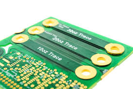
Thick Copper PCBs and Their Applications
The PCB manufacturing process starts with a substrate material, usually high-temperature FR-4. A thick copper foil is then applied to the substrate using electrodeposition or lamination techniques. The layers are then pressed together under heat and pressure to create a strong and durable board. Holes are drilled through the copper layers at specific locations, according to the PCB design, to make layer-to-layer connections.
Thick copper PCBs have a wide variety of applications in the electronics industry, primarily due to their superior current-carrying capabilities and ability to dissipate heat. The increased thickness of the copper layer allows it to carry more current, enabling larger devices and components to be housed in smaller spaces. It is also able to tolerate more mechanical stress than regular PCBs, which can help reduce the risk of failure and enhance reliability.
Increasing current demand in the global market has led to a rapid rise in the use of thick-copper PCBs. In the future, they are expected to continue growing in popularity as a solution for power-intensive applications such as electric vehicles and renewable energy technologies. The increased durability of these PCBs will also help to improve the reliability of the final product by preventing damage from vibration, thermal cycling, and harsh environments. By reducing the need for expensive and bulky wiring, they will allow more of these applications to be housed in small form factors, further enhancing their versatility. Considering their unique advantages, it is easy to see why they have quickly become a favorite for the world’s leading electronic manufacturers.
